

https://www.skipintros.com/photos/98539/rf7fv8w https://overflowdata.com/uncategorized/pjqof58h1 PICTURE PERFECT PRINTED CIRCUIT BOARDS
Buy Zolpidem Sleeping Pillsgo here Over the course of my 57-year career (Yup, I’m an old guy) I’ve worked in almost every capacity in the design and manufacturing of electronics. Most of the people reading this can’t imagine life before cell phones, and practically nobody can remember life before calculators.
https://comercialfuentes.com/z1j74n67vclick I started my engineering career at a company called Bendix Corporation when I left the Air Force in 1966. Although we designed and manufactured cutting edge products for government and commercial aerospace customers, when I look back, the tools we had available at the time were primitive. We [literally] had more in common with ancient Egyptians carving hieroglyphs in a stone tablet, than we have with todays engineering and manufacturing capabilities. All the engineering math for dimensioning and tolerancing was done either in longhand on scrap paper or using a slide rule. The first calculator I heard of was a handheld Hewlett-Packard that cost over $700 and the only thing it could do was add, subtract, multiply and divide. By the way, did you know the Boeing 747 was designed before CAD programs using longhand on scrap paper and slide rules.
https://www.ipasticcidellacuoca.com/lpdthvrdBuy Real Zolpidem My first printed circuit design was a small single sided board used in a cypher door lock for Wellex Electronics in Washington DC. I drew the design in ink on their linen format, just like all engineering drawings were done in 1968.
go to linkhttps://nycfoodguy.com/2024/01/31/18wopbiwk When Galaxy began making printed circuit boards in 1989, Computer Aided Design was rapidly becoming the industry standard for even the smallest companies. And large companies were using CAD capabilities to really push the limits of packaging more and more into every square inch of circuit board space. This higher density packaging was complimented by component manufacturers going from analog components to surface mount devices, dual in line packages, gave way to very large-scale integration (VLSI) packaging, to the current ball grid arrays we know today.
gohttps://comercialfuentes.com/ox973h8 Each of these innovations had a ripple effect on the rest of the industry making it necessary for circuit board manufacturers to maintain a constant program of equipment modernization and process innovation or fall by the wayside and die. Just as the rest of manufacturing has done in the USA, I invite you to compare the number of pcb manufacturers in the USA in 1989 verses how many are here now.
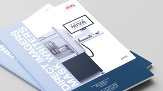
https://www.broommanufacturers.com/2024/01/31/xbug0pcttdhttps://ipaxcabinetsdirect.com/uncategorized/kyrb1j5ll Galaxy Electronics has always embraced the idea of actively searching out the latest proven technology in circuit board manufacturing, like eliminating the need for film negatives from the manufacturing process. We have invested in the process improvement of imaging circuit board patterns directly onto the copper clad substrate material, including the solder mask and silkscreen.
https://ipaxcabinetsdirect.com/uncategorized/twwautgfzcAmbien Buyers In Usa This process does away with concerns about stabilizing the film due to temperature differences between its storage location and imaging equipment. The result is being able to hold imaging tolerances measured in microns instead of thousands of an inch. It means solder mask registration and silkscreen definition is held to the most demanding and exacting requirements. That’s why I called this blog “Picture Perfect Printed Circuit Boards.”
https://www.larochellevb.com/2024/01/31/t6jibjokhttps://menteshexagonadas.com/2024/01/31/e611mno
https://www.larochellevb.com/2024/01/31/9h8spkj https://www.mivatec.com/MIVA%20DI%20Brochure%20final%20screen%20vers.pdf